- 您现在的位置:买卖IC网 > Sheet目录2007 > LTC6994CDCB-2#TRPBF (Linear Technology)IC DELAY LINE 6-DFN
LTC6994-1/LTC6994-2
14
699412fb
operaTion
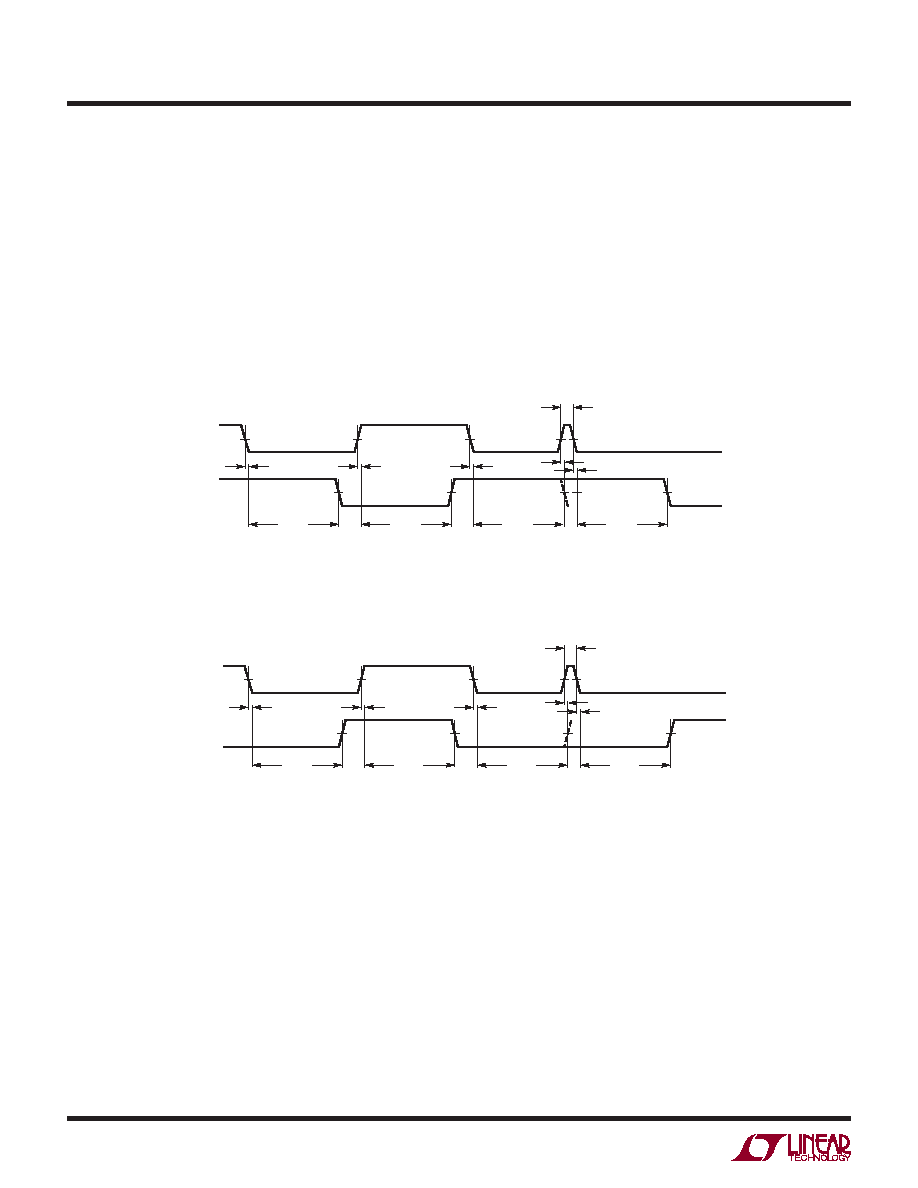
LTC6994-2 Functionality
Figures 5 details the basic operation of the LTC6994-2
when configured for noninverting operation (POL = 0). As
before, a rising edge on the IN pin initiates the timing and,
if IN remains high, OUT will transition high after tDELAY.
UnliketheLTC6994-1,fallingedgesaredelayedinthesame
way. When IN transitions low, OUT will follow after tDELAY.
If the input doesn’t remain high or low long enough for
OUT to follow, the timing will restart on the next transition.
Also unlike the LTC6994-1, the output pulse width can
never be less than tDELAY. Therefore, the LTC6994-2 can
generate pulses with a defined minimum width.
Figure 6 details the operation of the LTC6994-2 when the
output is inverted (POL = 1).
Figure 5. Both Edges Delayed Timing Diagram (LTC6994-2, POL = 0)
Figure 6. Both Edges Delayed (Inverting) Timing Diagram (LTC6994-2, POL = 1)
IN
OUT
tDELAY
tPD
tWIDTH
tPD
tDELAY
tPD
tDELAY
699412 F05
IN
OUT
tDELAY
tPD
tWIDTH
tDELAY
699412 F06
发布紧急采购,3分钟左右您将得到回复。
相关PDF资料
LTC7541ABN#PBF
IC CMOS D/A CONV 12BIT 18-DIP
LTC7545ACG#TRPBF
IC D/ACONV MULTIPLY 12BIT 20SSOP
LTC8043EN8
IC D/A CONV 12BIT SERIAL 8-DIP
LTC8143ESW#TRPBF
IC D/A CONV 12BIT SERIAL 16-SOIC
LTM9011CY-14#PBF
IC ADC 14BIT UMODULE 140BGA
LV5609LP-E
IC CLOCK DRIVER VERTICAL 24VCT
LV5609LP-TE-L-E
IC CLOCK DRIVER VERT VCT24
M-986-2A1PL
IC TRANSCEIVER MF 2CHAN 44-PLCC
相关代理商/技术参数
LTC6994CDCB-2TRMPBF
制造商:LINER 制造商全称:Linear Technology 功能描述:TimerBlox: Delay Block/ Debouncer
LTC6994CS6-1#PBF
制造商:Linear Technology 功能描述:SC-Timing, Cut Tape Delay with Rising or Falling Edge Trigger
LTC6994CS6-1#TRMPBF
功能描述:IC DELAY LINE TSOT-23-6 RoHS:是 类别:集成电路 (IC) >> 时钟/计时 - 延迟线 系列:TimerBlox® 标准包装:2,500 系列:- 标片/步级数:- 功能:多个,不可编程 延迟到第一抽头:10ns 接头增量:- 可用的总延迟:10ns 独立延迟数:4 电源电压:4.75 V ~ 5.25 V 工作温度:0°C ~ 70°C 安装类型:表面贴装 封装/外壳:14-SOIC(0.154",3.90mm 宽) 供应商设备封装:14-SOIC 包装:带卷 (TR)
LTC6994CS6-1#TRPBF
功能描述:IC DELAY LINE TSOT-23-6 RoHS:是 类别:集成电路 (IC) >> 时钟/计时 - 延迟线 系列:TimerBlox® 标准包装:2,500 系列:- 标片/步级数:- 功能:多个,不可编程 延迟到第一抽头:10ns 接头增量:- 可用的总延迟:10ns 独立延迟数:4 电源电压:4.75 V ~ 5.25 V 工作温度:0°C ~ 70°C 安装类型:表面贴装 封装/外壳:14-SOIC(0.154",3.90mm 宽) 供应商设备封装:14-SOIC 包装:带卷 (TR)
LTC6994CS6-1TRMPBF
制造商:Linear Technology 功能描述:Delay Block/Debouncer 1us-33.6s TSOT23-6
LTC6994CS6-2#PBF
制造商:Linear Technology 功能描述:DELAY BLOCK/DEBOUNCER 5.5V T 制造商:Linear Technology 功能描述:DELAY BLOCK/DEBOUNCER, 5.5V, TSOT-23-6; Operating Mode:Monostable; Supply Voltage Min:2.25V; Supply Voltage Max:5.5V; Digital IC Case Style:TSOT-23; No. of Pins:6; Clock External Input:Yes; Operating Temperature Min:0C ;RoHS Compliant: Yes
LTC6994CS6-2#TRMPBF
功能描述:IC DELAY LINE TSOT-23-6 RoHS:是 类别:集成电路 (IC) >> 时钟/计时 - 延迟线 系列:TimerBlox® 标准包装:2,500 系列:- 标片/步级数:- 功能:多个,不可编程 延迟到第一抽头:10ns 接头增量:- 可用的总延迟:10ns 独立延迟数:4 电源电压:4.75 V ~ 5.25 V 工作温度:0°C ~ 70°C 安装类型:表面贴装 封装/外壳:14-SOIC(0.154",3.90mm 宽) 供应商设备封装:14-SOIC 包装:带卷 (TR)
LTC6994CS6-2#TRPBF
功能描述:IC DELAY LINE TSOT-23-6 RoHS:是 类别:集成电路 (IC) >> 时钟/计时 - 延迟线 系列:TimerBlox® 标准包装:2,500 系列:- 标片/步级数:- 功能:多个,不可编程 延迟到第一抽头:10ns 接头增量:- 可用的总延迟:10ns 独立延迟数:4 电源电压:4.75 V ~ 5.25 V 工作温度:0°C ~ 70°C 安装类型:表面贴装 封装/外壳:14-SOIC(0.154",3.90mm 宽) 供应商设备封装:14-SOIC 包装:带卷 (TR)